Wall Moisture Sensor - WSM1 v1.2.0
Monitor wall moisture using capacitive sensors. The device supports two methods for reading capacitive values, allowing for comparison and experimentation.
Table of Contents
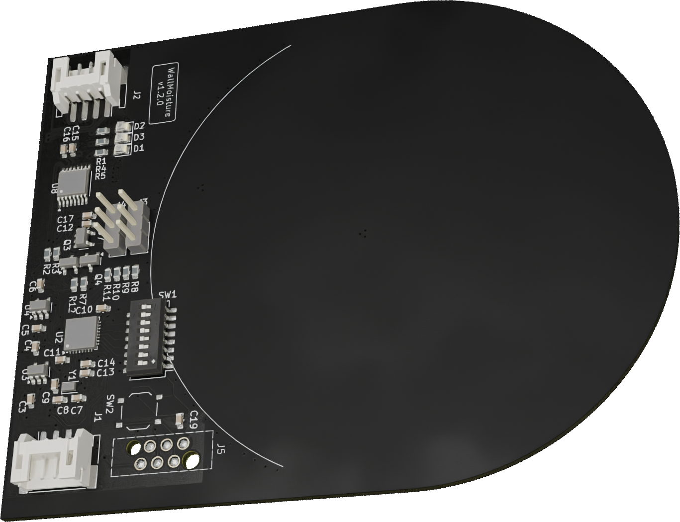
Render Top Angled
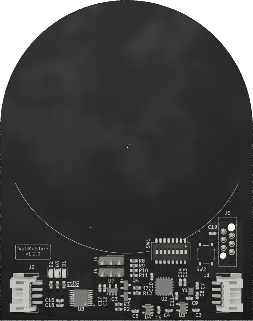
Render Top
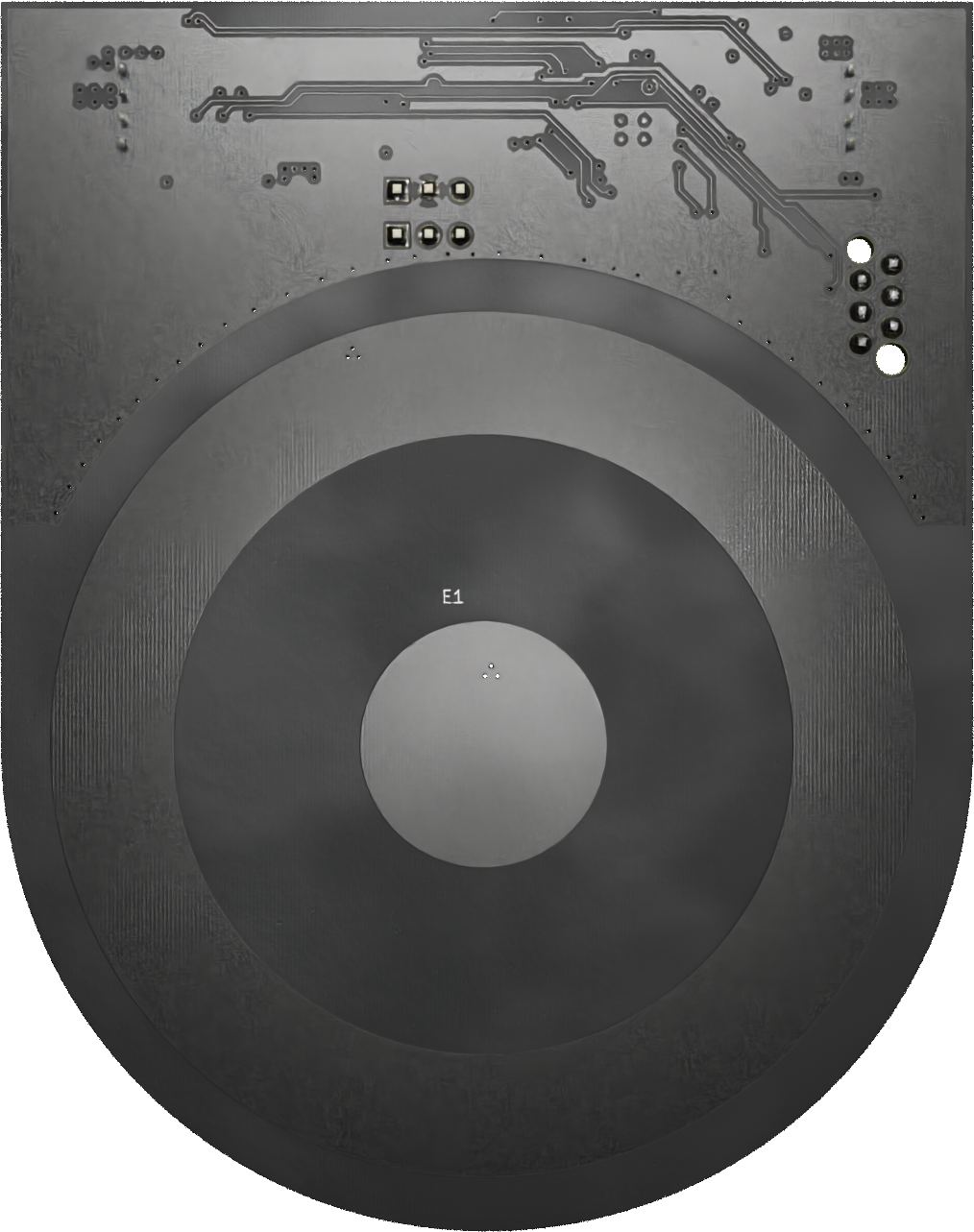
Render Bottom
Schematic
Layout
Interactive BOM
BOM
KiCad Revision Inspector (KiRI)
KiCad Revision Inspector (KiRI) is a tool for comparing different versions of KiCad projects. It exports project revisions to SVG format for visual comparison using an onion skin view. This helps identify changes and errors in PCB designs.
Light
Dark
Downloads
jlcpcb
3D Step
Reports
ERC Report
- Errors: 0
- Warnings: 0
- Link: HTML Report
DRC Report
- Errors: 7
- Warnings: 2
- Link: HTML Report
PCB
Board size: 78.5x99.34 mm (3.09x3.91 inches)
- This is the size of the rectangle that contains the board
- Thickness: 1.6 mm (63 mils)
- Material: FR4
- Finish: ENIG
- Layers: 4
- Copper thickness: 35 µm
Solder mask: TOP / BOTTOM
- Color: Black
Silk screen: TOP / BOTTOM
- Color: White
Stackup:
| Name | Type | Color | Thickness [µm] | Material | Er | Loss tan |
|---|---|---|---|---|---|---|
| F.SilkS | Top Silk Screen | |||||
| F.Paste | Top Solder Paste | |||||
| F.Mask | Top Solder Mask | 10 | ||||
| F.Cu | copper | 35 | ||||
| dielectric 1 | prepreg | 100 | FR4 | 4.5 | 0.020 | |
| In1.Cu | copper | 35 | ||||
| dielectric 2 | core | 1240 | FR4 | 4.5 | 0.020 | |
| In2.Cu | copper | 35 | ||||
| dielectric 3 | prepreg | 100 | FR4 | 4.5 | 0.020 | |
| B.Cu | copper | 35 | ||||
| B.Mask | Bottom Solder Mask | 10 | ||||
| B.Paste | Bottom Solder Paste | |||||
| B.SilkS | Bottom Silk Screen |
Important sizes
Clearance: 0.2 mm (8 mils)
Track width: 0.2 mm (8 mils)
- By design rules: 0.1 mm (4 mils)
Drill: 0.4 mm (16 mils)
- Vias: 0.4 mm (16 mils) [Design: 0.4 mm (16 mils)]
- Pads: 1.1 mm (43 mils)
- The above values are real drill sizes, they add 0.1 mm (4 mils) to plated holes (PTH)
Via: 0.6/0.3 mm (24/12 mils)
- By design rules: 0.25/0.3 mm (10/12 mils)
- Micro via: yes [0.2/0.1 mm (8/4 mils)]
- Buried/blind via: yes
- Total: 139 (thru: 139 buried/blind: 0 micro: 0)
Outer Annular Ring: 0.1 mm (4 mils)
- By design rules: 0.13 mm (5 mils)
Eurocircuits class: 8C
- Using min drill 0.4 mm for an OAR of 0.1 mm
General stats
Components count: (SMD/THT)
- Top: 43/2 (SMD + THT)
- Bottom: 1/0 (SMD)
Defined tracks:
- 0.2 mm (8 mils)
- 0.4 mm (16 mils)
- 0.8 mm (31 mils)
Used tracks:
- 0.2 mm (8 mils) (459) defined: yes
- 0.4 mm (16 mils) (77) defined: yes
- 0.8 mm (31 mils) (1) defined: yes
Defined vias:
Used vias:
- 0.6/0.3 mm (24/12 mils) (Count: 139, Aspect: 2.7 A) defined: no
Holes (excluding vias):
- 1.0 mm (39 mils) (6)
- 1.5 mm (59 mils) (6)
- 2.2 mm (87 mils) (1)
- 2.6 mm (102 mils) (1)
Oval holes:
Drill tools (including vias and computing adjusts and rounding):
- 0.4 mm (16 mils) (139)
- 1.1 mm (43 mils) (6)
- 1.6 mm (63 mils) (6)
- 2.2 mm (87 mils) (1)
- 2.6 mm (102 mils) (1)
Solder paste stats:
Using a paste with 87.75 % alloy, that has an specific gravity for the alloy of 7.4 g/cm³ and 1.0 g/cm³ for the flux. This paste has an specific gravity of 4.15 g/cm³.
The stencil thickness is 0.12 mm.
| Side | Pads with paste | Area [mm²] | Paste [g] |
|---|---|---|---|
| Total | 172 | 173.54 | 0.86 |
Note: this is just an approximation to the theoretical value. Margins of the solder mask and waste aren’t computed.